Online PCB design & circuit simulator
Table Of Content
This does not include the KiCad source code, libraries, documentation, and any third party tools or products mentioned on the website. Allegro X Design Platform, from Cadence Design System, offers engineers a system design platform that integrates logic/physical design, system analysis, and design data management for PCB and system design. Designed to accelerate, simplify and improve the handoff process from design to production.
Source Data Fig. 3
An Arduino EEPROM reader PCB design #PCB #Arduino @diyelectromusic « Adafruit Industries – Makers, hackers ... - Adafruit Blog
An Arduino EEPROM reader PCB design #PCB #Arduino @diyelectromusic « Adafruit Industries – Makers, hackers ....
Posted: Thu, 29 Feb 2024 08:00:00 GMT [source]
You can have your components automatically arranged or you can place them manually. You can also use these options together, which allows you to take advantage of the speed of auto-placement and ensure your board is laid out according to good component placement guidelines. An added advanced feature of this latest version of Altium Designer is the ability to arrange components as groups. You can define these groups in the PCB layout, or you can define groups on the schematic using Cross Select Mode, which is accessible from the Tools menu. The last point above is quite important, as complex designs may use hierarchical schematics.
The Tool of Choicefor PCB DesignersWorldwide
Using a systematic approach such as this ensures that all aspects of your circuit board design are accounted for inherently during the process, with minimal need to retrace your steps. Your preferences here should be guided by the design for manufacturing (DFM) specifications of your PCB manufacturer. If you already defined your PCB DFM requirements as design rules (see Step 5), Altium Designer will automatically check these rules as you place vias, drill holes, pads, and traces in your layout. Altium Designer provides a great deal of flexibility and allows you to quickly place components on your circuit board.
How to Design a PCB Layout
But most importantly, we use our knowledge of methods and approaches to electric circuit design that we've accumulated over years of work. Every PCB will need to have a clear ground connection so that all components in the design will form complete circuits and so that electrical power will be supplied throughout the design. The ground connection can be to a battery on the board or to an external power supply. No matter how that connection is made, that ground connection then needs to be supplied to all other components in the PCB. By far, the easiest way to do this is with a ground plane, where one of the layers in the PCB is used for ground with a large sheet of copper covering the entire layer.
Simple task automation.
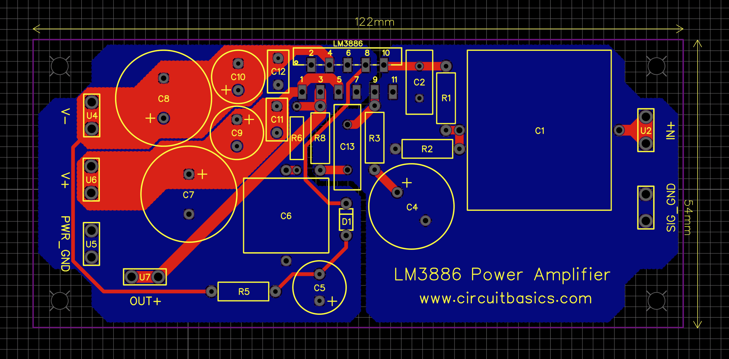
We often use silkscreen labels to indicate what the function of each pin or LED. Soldermask is most commonly green in color but nearly any color is possible. We use red for almost all the SparkFun boards, white for the IOIO board, and purple for the LilyPad boards. The copper thickness can vary and is specified by weight, in ounces per square foot. The vast majority of PCBs have 1 ounce of copper per square foot but some PCBs that handle very high power may use 2 or 3 ounce copper. Each ounce per square translates to about 35 micrometers or 1.4 thousandths of an inch of thickness of copper.
Once you’ve placed your components and any other mechanical elements, you’re ready to route your traces in this PCB design step. As you route your board, try to come up with a strategy to finish your important routes first, then fill in the gaps with the remaining connections as needed. Some of the important routes will include your power nets, any impedance-controlled nets, and any noise-sensitive nets like low-level analog signals. Be sure to utilize good routing guidelines and take advantage of Altium Designer tools to simplify the process, such as highlighting nets and interactive routing features. After you’ve learned about the manufacturing process, as well as some of the standard capabilities found from PCB fabricators, it will be much easier to understand some of the limits imposed in design rules.
What Kind of Education is Required to be a PCB Designer?
Once your board has passed the final DRC, you need to generate the design files for your manufacturer. The design files should include all the information and data necessary to build your board; including any notes or special requirements to ensure that your manufacturer is clear on what you require. For most manufacturers, you will be able to use a set of Gerber files as shown below; however, some manufacturers prefer other manufacturing file formats (IPC-2581 or ODB++). Before routing your traces, it is a good idea to place your drill holes (mounting and vias). If your circuit board design is complicated you may need to modify at least some of the via locations during trace routing. This can be done easily from the via Properties dialog, shown below.
Step 6: PCB Assembly – Soldering the Components to the Board
Their recycling is challenging due to their use of irreversibly cured thermoset epoxies in manufacturing. Here, to tackle this challenge, we present a PCB formulation using transesterification vitrimers (vPCBs) and an end-to-end fabrication process compatible with standard manufacturing ecosystems. Our cradle-to-cradle life-cycle assessment shows substantial environmental impact reduction of the vPCBs over conventional PCBs in 11 categories. We successfully manufactured functional prototypes of Internet of Things devices transmitting 2.4 GHz radio signals on vPCBs with electrical and mechanical properties meeting industry standards. Fractures and holes in vPCBs are repairable while retaining comparable performance over multiple repair cycles.
1) To rearrange an existing route drag the segment by clicking once to select the segment, position the mouse over the segment to display the quad-arrow cursor, then click and hold to start dragging that segment. If you click Finish before completing the entire Wizard, the newwidth rule will be created using the system defaults for the component type you selected. 10) Exit part placement by clicking the Right Mouse Button or pressing the ESC key. 7) Referring to the rough schematic diagram shown before, notice that Q2 is drawn as a mirror of Q1. To flip the orientation of the transistor that is floating on the cursor, press the X key on the keyboard. 4) Before placing the part on the schematic, press the Tab key to open the properties panel and pause placement.
5) Using the image below as a guide, position and place the two capacitors in the same way that you placed the previous parts. IntLib library, which should already be selected in the Libraries panel. To position the component more accurately, press the PageUp keytwice to zoom in two steps. 2) Find the 2N3904 transistor in the panel by either scrolling through the component list or by using the search button. Refer to the rough schematic sketch above for the general layout of the circuit, and place 2N3904 transistors Q1 and Q2. Choose or create the project directory and save the project withthe name Multivibrator.

The rules have been previously configured for this tutorial and the design is ready to be validated. If you’ve ever used a new piece of software, you know about the learning curve involved. With so many different PCB design packages on the market, getting up to speed quickly requires design software that places all of your critical design tools in a single interface. Why not purchase PCB design software that shows you how to be successful? Other design software platforms claim to integrate features, but they still separate critical design tools into addons without providing the guidance new users need to be successful. Instead, you should use design software that gathers all your design tools in one place alongside design resources.
Circuitmaker is a unique combination of the broad design community, a free PCB Design software and services, that allow everyone to work on the same premise and share the knowledge with ease. We know, to turn great ideas into real products, you need design tools that won’t limit your imagination or hold you back. The CircuitMaker PCB Design Editor has all the power you need to design high quality schematics and layout, with no artificial limits on layer counts or board area. Once you’ve determined your device requirements for your application, Altium Designer allows you to encode these specifications in design rules. You can rest assured your layout will comply with your design rules, and you can check and correct any rules violations quickly and easily. These rule definition and checking features help you stay within standard design guidelines and help you build a device that meets your technical requirements.
Altium Designer uses a rules-based design that helps you avoid simple mistakes. If you’re new to PCB design or you’re new to Altium Designer, the intuitive interface allows you to start designing schematics from the moment the program starts. Capturing your schematic in your layout is simple, allowing you to start routing connections between components and finish building your new device. All along, the rules-driven design engine, PCB design tutorial, and online resources will help you stay on track. After you’ve created your schematic, for the next PCB design step you’ll need to use the schematic capture tool in Altium Designer to import components into a blank PCB layout. First, create a blank printed circuit board document which will generate a PcbDoc file.
We have only scratched the surface of what is possible to do with Altium Designer on Altium 365. You can check the product page for a more in-depth feature description or one of the On-Demand Webinars. Simple, intuitive, well-known user-interface concepts help to get startedwith LibrePCB very quickly. No need to study the documentation for days –just start working with it.


Comments
Post a Comment